Exploring a GreenPAK SLG46826 (Part 1)
GreenPAK from RENESAS are small package SMDs that contain a number of route-able digital and analog functional blocks. There is some similarity with a CPLD/FPGA, but the range of blocks is more diverse and there is no HDL. GreenPAKs are configured and programmed via RENESAS’ free to use software Go_Configure, with the developer connecting the inputs and outputs of the blocks to implement their design. When combined with their advanced development board, it feels to me a lot like a virtual equivalent of prototyping with discrete logic chips, but without the physical reality of having to maintain an inventory. The end result takes up a lot less PCB real estate too, which is obviously a major selling point. Once the design is finalised it is programmed into the GreenPAK’s non volatile memory (nvm). When the GreenPAK powers up, the design in nvm is copied into the GreenPAK’s ram to “run”. I’ve used them successfully in a few of my projects.
However, the vast majority of GreenPAKs are one time programmable (OTP). Good for economy with large production runs, and I’m sure, good for other reasons too. OTP does focus the mind, but it’s too late to change your mind once you have programmed the chip. My ultimate objective is use a GreenPAK as a companion chip to an mcu, perhaps a homegrown one, which is why the SLG46826 (and also the SLG47004, as its analog focus would make my homegrown effort more useful) are interesting to me. They have many time programmable (MTP) nvm, and both nvm and ram are readable and writable over I2C. This is valuable in my use case as it may allow me to configure my companion GreenPak directly from my mcu (in Forth, hopefully).
However, before I get ahead of myself, I need to see whether I really can dynamically configure these GreenPAKs over I2C, which gives a great excuse to dig out an UNO compatible and flash AmForth onto it. AmForth makes a great swiss army knife of a tool for investigating other devices.
Part 1 - The road to blinky
Aim of this session is to get some kind of led flashing by dynamically configuring the ram of a factory fresh SLG46826. Not original, but if I can’t do that then any grander notions are out the window. I’ve concatenated a few hours of tinkering into one continuous amforth-shell session and then annotated it. That way, I know what gets written here was indeed what got run.
Start off by using anew so that future #include of the file don’t clog up mcu flash.
S|     1|anew _op1_
W|     2|
The large prebuilt hex file has AmForth’s standard I2C words plus a few more to make things easier. Init with a 100kHz clock and scan the I2C bus for hardware addresses.
|S|    3|i2c.100k
|W|    4|
|S|    5|i2c.detect
|O|    5|      0  1  2  3  4  5  6  7  8  9  A  B  C  D  E  F
|O|    5| 0:                       --  8  9  A  B -- -- -- --
|O|    5|10:  -- -- -- -- -- -- -- -- -- -- -- -- -- -- -- --
|O|    5|20:  -- -- -- -- -- -- -- -- -- -- -- -- -- -- -- --
|O|    5|30:  -- -- -- -- -- -- -- -- -- -- -- -- -- -- -- --
|O|    5|40:  -- -- -- -- -- -- -- -- -- -- -- -- -- -- -- --
|O|    5|50:  -- -- -- -- -- -- -- -- -- -- -- -- -- -- -- --
|O|    5|60:  -- -- -- -- -- -- -- -- -- -- -- -- -- -- -- --
|O|    5|70:  -- -- -- -- -- -- -- --
|W|    6|
There’s only one device on the I2C bus, but we have 4 hardware addresses. The datasheet and programming guide show three areas of memory; ram (256B), nvm (256B) and eeprom (256B), each accessed via their own I2C hardware address. In this case $8 for ram, $a for nvm and $b for eeprom. A little Forth to have a look at the nvm and ram in more detail.
|S|    7|$8 Rvalue ram
|S|    8|$a Rvalue nvm
|S|    9|$b Rvalue eep
|W|   10|
|S|   11|: h2. ( u -- ) base @ >r hex 0 <# # # #> type space r> base ! ;
|S|   12|: b. base @ >r bin 0 <# $10 0 do # loop #> type space r> base ! ;
|W|   13|
|S|   14|: gpak.rule ( n -- ) 0 ?do [char] - emit loop ;
|S|   15|: gpak.show ( n -- )
|S|   16|    a> >r \ put a on R
|S|   17|    >a
|C|   18|    \ header
|S|   19|    cr s" nn | " itype $10 0 do i h2. loop cr #52 gpak.rule cr
|C|   20|    \ #256 byte page
|S|   21|    $10 0 do
|S|   22|        i $10 * h2. [char] | emit space
|S|   23|        $10 0 do
|S|   24|             1 i j $10 * + 1 a> i2c.m!n@ h2.
|S|   25|        loop
|S|   26|        cr
|S|   27|    loop
|S|   28|    r> >a \ get a back from R
|S|   29|;
|W|   30|
At power on nvm is copied (fully?) to ram. The two memory dumps are very similar but there are differences. However, the ram dump is from a live system - so some of the bytes may reflect the live state of the system rather than its static factory configuration. A more detailed study of register map in datasheet is next thing on the list.
|S|   31|nvm gpak.show
|O|   31|
|O|   31|nn | 00 01 02 03 04 05 06 07 08 09 0A 0B 0C 0D 0E 0F
|O|   31|----------------------------------------------------
|O|   31|00 | 00 00 00 00 00 00 00 00 00 00 00 00 00 00 00 00
|O|   31|10 | 00 00 00 00 00 00 00 00 00 00 00 00 00 00 00 00
|O|   31|20 | 00 00 00 00 00 00 00 00 00 00 00 00 00 00 00 00
|O|   31|30 | 00 00 00 00 00 00 00 00 00 00 00 00 00 00 00 00
|O|   31|40 | 00 00 00 00 00 00 00 00 00 00 00 00 00 00 00 00
|O|   31|50 | 00 00 00 00 00 00 00 00 00 00 00 00 00 00 00 00
|O|   31|60 | 00 00 00 00 00 00 00 00 00 00 00 00 00 00 00 00
|O|   31|70 | 00 00 00 00 00 00 00 00 00 00 00 00 00 00 00 00
|O|   31|80 | 00 00 00 00 00 00 00 00 00 00 00 00 00 00 00 00
|O|   31|90 | 00 00 00 00 00 00 00 00 00 00 00 00 00 00 00 00
|O|   31|A0 | 00 00 00 00 00 00 00 00 00 00 00 00 00 00 00 00
|O|   31|B0 | 00 00 00 00 00 00 00 00 00 00 00 00 00 00 00 00
|O|   31|C0 | 00 00 00 00 00 00 00 00 00 00 01 00 00 00 0E 00
|O|   31|D0 | 00 00 00 00 00 00 00 00 00 00 00 00 00 00 00 00
|O|   31|E0 | 00 00 00 00 00 00 00 00 00 00 00 00 00 00 00 00
|O|   31|F0 | 41 14 10 29 26 21 10 00 00 00 B8 00 00 00 00 A5
|W|   32|
|S|   33|ram gpak.show
|O|   33|
|O|   33|nn | 00 01 02 03 04 05 06 07 08 09 0A 0B 0C 0D 0E 0F
|O|   33|----------------------------------------------------
|O|   33|00 | 00 00 00 00 00 00 00 00 00 00 00 00 00 00 00 00
|O|   33|10 | 00 00 00 00 00 00 00 00 00 00 00 00 00 00 00 00
|O|   33|20 | 00 00 00 00 00 00 00 00 00 00 00 00 00 00 00 00
|O|   33|30 | 00 00 00 00 00 00 00 00 00 00 00 00 00 00 00 00
|O|   33|40 | 00 00 00 00 00 00 00 00 00 00 00 00 00 00 00 00
|O|   33|50 | 00 00 00 00 00 00 00 00 00 00 00 00 00 00 00 00
|O|   33|60 | 00 00 00 00 00 00 00 00 00 00 00 00 00 00 00 00
|O|   33|70 | 00 00 00 00 00 20 00 00 01 00 00 C0 00 00 00 00
|O|   33|80 | 00 00 00 00 00 00 00 00 00 00 00 00 00 00 00 00
|O|   33|90 | 00 00 00 00 00 00 00 00 00 00 00 00 00 00 00 00
|O|   33|A0 | 00 00 00 00 00 00 00 00 00 00 00 00 00 00 00 00
|O|   33|B0 | 00 00 00 00 00 00 00 00 00 00 00 00 00 00 00 00
|O|   33|C0 | 00 00 00 00 00 00 00 00 00 00 01 00 00 00 0E 00
|O|   33|D0 | 00 00 00 00 00 00 00 00 00 00 00 00 00 00 00 00
|O|   33|E0 | 00 00 00 00 00 00 00 00 00 00 00 00 00 00 00 00
|O|   33|F0 | 41 14 10 29 26 21 10 FF FF 02 B8 06 84 00 00 A5
|W|   34|
The datasheet notes that byte $ca is the one responsible for determining the I2C address of the device via a mapping arrangement (clearly, as [$ca]=$01 has to arrive at $8, $a and $b). The datasheet is very clear about how this is done, but since the device “runs” out of ram lets write some words to read and write a byte of ram and use them to change the contents of $ca and see what happens.
|S|   35|: ram! ( c c-addr --   ) 2 ram i2c.n! ;
|S|   36|: ram@ (   c-addt -- c ) >r 1 r> 1 ram i2c.m!n@ ;
|W|   37|
|S|   38|$ca ram@ .
|O|   38|1
|W|   39|
|S|   40|2 $ca ram!
|W|   41|
|S|   42|i2c.detect
|O|   42|      0  1  2  3  4  5  6  7  8  9  A  B  C  D  E  F
|O|   42| 0:                       -- -- -- -- -- -- -- -- --
|O|   42|10:  10 11 12 13 -- -- -- -- -- -- -- -- -- -- -- --
|O|   42|20:  -- -- -- -- -- -- -- -- -- -- -- -- -- -- -- --
|O|   42|30:  -- -- -- -- -- -- -- -- -- -- -- -- -- -- -- --
|O|   42|40:  -- -- -- -- -- -- -- -- -- -- -- -- -- -- -- --
|O|   42|50:  -- -- -- -- -- -- -- -- -- -- -- -- -- -- -- --
|O|   42|60:  -- -- -- -- -- -- -- -- -- -- -- -- -- -- -- --
|O|   42|70:  -- -- -- -- -- -- -- --
As expected. Device now has a different block of I2C hardware addresses… and my values ram, nvm and eep are pointing to the wrong places. Write a Forth word to scan the I2C bus for possible SLG46826 devices (using the specified mapping arrangement) and assign the values ram, nvm and eep based on the first one found.
|W|   43|
|S|   44|false Rvalue gpak.set?
|W|   45|
|S|   46| : gpak.set ( u -- )
|S|   47|    3 lshift dup to ram
|S|   48|    1+ 1+ dup to nvm
|S|   49|    1+ to eep
|S|   50|;
|W|   51|
|S|   52|: gpak.scan ( -- )
|S|   53|    a> >r
|W|   54|
|S|   55|    false to gpak.set?
|W|   56|
|S|   57|    s" ctl ram     nvm eep" itype cr
|S|   58|    s" --- --- --- --- ---" itype cr
|W|   59|
|S|   60|    $10 0 do
|S|   61|        i h2. space
|S|   62|        i 3 lshift       \ hwd --
|S|   63|        dup i2c.ping? if
|S|   64|            0 >a
|S|   65|            4 0 do
|S|   66|                dup i + i2c.ping? if
|S|   67|                    a> 1+ >a dup i + h2. space
|S|   68|                then
|S|   69|            loop
|S|   70|            drop
|S|   71|            a> 4 = gpak.set? not and if
|S|   72|                i gpak.set true to gpak.set?
|S|   73|                [char] * emit
|S|   74|            then
|S|   75|        else
|S|   76|            drop
|S|   77|        then
|S|   78|        cr
|S|   79|    loop
|S|   80|    r> >a
|S|   81|;
|W|   82|
I’ve only got one device, but it has found it and assigned the values (10 is in hex so ram is 16 in decimal).
|S|   83|gpak.scan
|O|   83|ctl ram     nvm eep
|O|   83|--- --- --- --- ---
|O|   83|00
|O|   83|01
|O|   83|02  10  11  12  13  *
|O|   83|03
|O|   83|04
|O|   83|05
|O|   83|06
|O|   83|07
|O|   83|08
|O|   83|09
|O|   83|0A
|O|   83|0B
|O|   83|0C
|O|   83|0D
|O|   83|0E
|O|   83|0F
|W|   84|
|S|   85|ram .
|O|   85|16
|W|   86|
Time to move on to trying to configure the device (in ram), albeit in the most modest of ways.
One matrix to rule them all
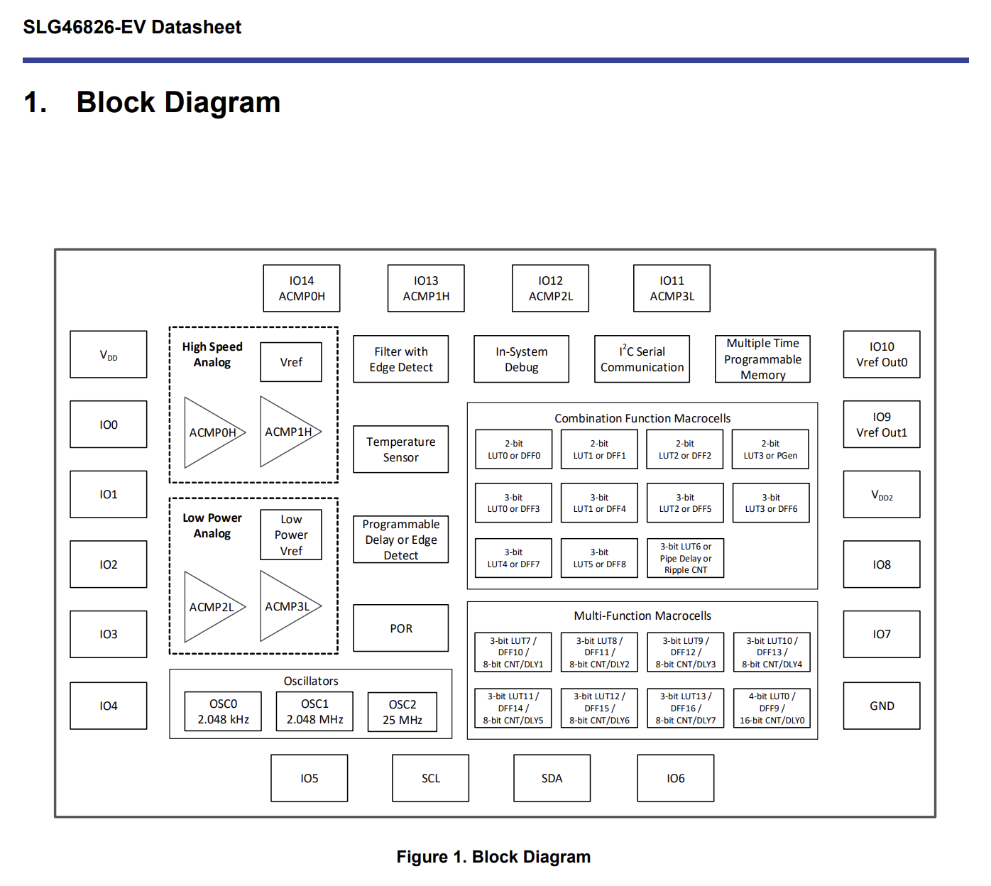
The functional block model of the device is shown clearly in Figure 1 on page 10 of the datasheet.
But how are these blocks connected? Enter the matrix. The matrix has input and outputs and these can be connected 1:n via I2C, so making the connections between functional blocks. But what are the matrix inputs and outputs? Matrix inputs are in fact block outputs and matrix outputs are in fact block inputs. From a matrix centric point of view this makes sense. All connections go through the matrix. There are 64 matrix inputs and 96 matrix outputs. To make a connection, a 6 bit [0..63] matrix input number is written to a 6 bit matrix output slot in ram. However the bit address of the output slot is not necessarily on a byte boundary. Matrix output slots form a bitstream, as do other elements of device configuration. Straight byte addressing should not be assumed!
So need a word to write a bit pattern b, over a mask m at a register bit address rb - bearing in mind that the memory slot at register bit address rb may span 2 bytes. With some made up addresses, I want a word that does this over I2C.
BYTE           $55       $54
RB        339..332  331..324
BEFORE    11111111  11111111

%0100 #330 %1111 rbm!

AFTER     11111101  00111111
This is what I came up with. Improvements welcomed.
|S|   87|: rbm! ( b rb m -- ) \ write bit pattern b over mask m starting at rb
|C|   88|    \ %0100 #330 %1111 rmb!
|W|   89|
|S|   90|    >r                           \ b r q --        R     m --
|S|   91|    8 /mod over over r> rot rot  \ b r q m r q --  R       --
|S|   92|    >r >r >r nip                 \ r q  --         R q r m --
|S|   93|    2 swap 1 ram                 \ b 2 q 1 ram --  R   q r --
|S|   94|    i2c.m!n@                     \ b [54] [55] --  R   q r --
|S|   95|    8 lshift or                  \         b n --  R   q r --
|S|   96|    dup b.
|S|   97|    r>      r@ lshift invert     \       b n A --  R   q r --
|S|   98|    and                          \         b m --  R   q r --
|S|   99|    swap r@ lshift               \         m O --  R   q r --
|S|  100|    or                           \           m --  R   q r --
|S|  101|    dup b. cr
|S|  102|    dup $ff00 and 8 rshift       \         m H --  R   q r --
|S|  103|    swap $ff and                 \         H L --  R   q r --
|S|  104|    r> drop                      \         H L --  R     q --
|S|  105|    r> 3 ram i2c.n!              \             --  R       --
|S|  106|;
After writing the word rbm! I found section 15.7.3 I2C Byte Write Bit Masking in the datasheet, but I can’t immediately see how that would help with writes over byte boundaries.
Writes to slots of bit length 1 through 8 are needed, so make them now ( rb8! not the same as ram!)
|W|  107|
|S|  108|: rb1! ( b rb -- )        %1 rbm! ;
|S|  109|: rb2! ( b rb -- )       %11 rbm! ;
|S|  110|: rb3! ( b rb -- )      %111 rbm! ;
|S|  111|: rb4! ( b rb -- )     %1111 rbm! ;
|S|  112|: rb5! ( b rb -- )    %11111 rbm! ;
|S|  113|: rb6! ( b rb -- )   %111111 rbm! ;
|S|  114|: rb7! ( b rb -- )  %1111111 rbm! ;
|S|  115|: rb8! ( b rb -- ) %11111111 rbm! ;
|W|  116|
I have enough Forth words to finally do some configuring for the blinky. This involves a fair bit of datasheet work. I’ve chosen GPIO block io7, which is attached to pin 12 on the breakout DIP. This is byte addressable and only needs $80 to be written to it to enable it as a push-pull output.
|S|  117|$6b  constant io7      \ gpio config byte
|W|  118|
I’ve connected an LED + series resistor to the pin 12, so now need to change the matrix configuration to drive it high and then low. This means writing the matrix input for vdd to matrix output slot for io7 and then writing the matrix input for gnd to matrix output slot for io7. Repeatedly.
Matrix inputs (which are block outputs) are just constants. So make it so.
|S|  119|#63  constant vdd_     \ matrix input (block output)
|S|  120|0    constant gnd_     \ matrix input (block output)
Matrix outputs (block inputs) are register bit address that always receive an unsigned 6 bit number. I can use <builds … does> with rb6! to make my embryonic configuration DSL a little more elegant.
|W|  121|
|S|  122|: _: ( n -- )  <builds , does> @i rb6! ;
|W|  123|
|S|  124|#462 _: _io7           \ matrix output (block input)
|W|  125|
Why the AAA_ and _BBB ? Because it fits my mental image of
   BLOCK    |    MATRIX    |    BLOCK
            |              |
AAA_ (out)  | (in)   (out) |  (in) _BBB
            |              |
So at least for an io block can have this, with the visual check that a ???_ must face a _???
u1 constant BBB
u2 BBB ram!

AAA_ _BBB
Back to the blink. An embarrassing omission from the large prebuilt hex file. To be fixed.
|S|  126|: ms ( u -- ) 0 ?do 1ms pause loop ;
|W|  127|
This is the final word.
|S|  128|: blink ( u -- )
|S|  129|    0 ?do
|S|  130|        vdd_ _io7
|S|  131|        500 ms
|S|  132|        gnd_ _io7
|S|  133|        500 ms
|S|  134|    loop
|S|  135|;
|W|  136|
Write $80 to io7 pin config and execute 4 led blinks. It works (no video) and I’ve left the debug resister bit writes in for now.
|S|  137|$80 io7 ram!
|W|  138|
|S|  139|4 blink

         \         before            after
|O|  139|0000000000000000 0000111111000000
|O|  139|0000111111000000 0000000000000000
|O|  139|0000000000000000 0000111111000000
|O|  139|0000111111000000 0000000000000000
|O|  139|0000000000000000 0000111111000000
|O|  139|0000111111000000 0000000000000000
|O|  139|0000000000000000 0000111111000000
|O|  139|0000111111000000 0000000000000000
|W|  140|
|W|  141|
A very primitive blinky, but one that does configure the matrix. The SLG46826 does have its own oscillator blocks, so can handle the timing without external help from the mcu. That, however, is for Part 2.